Simics provides a set of DML templates to assist in writing models for
PCIe compliant devices. The templates are available in
[simics]/src/devices/dml-lib/pcie/.
A typical endpoint device would use the pcie_endpoint
template. This template defines the pcie_config register bank which
simulates a Type 0 Configuration header. It also defines a connect for
the upstream target, implements the required interfaces, and handles the
mapping of resources defined in any base address registers.
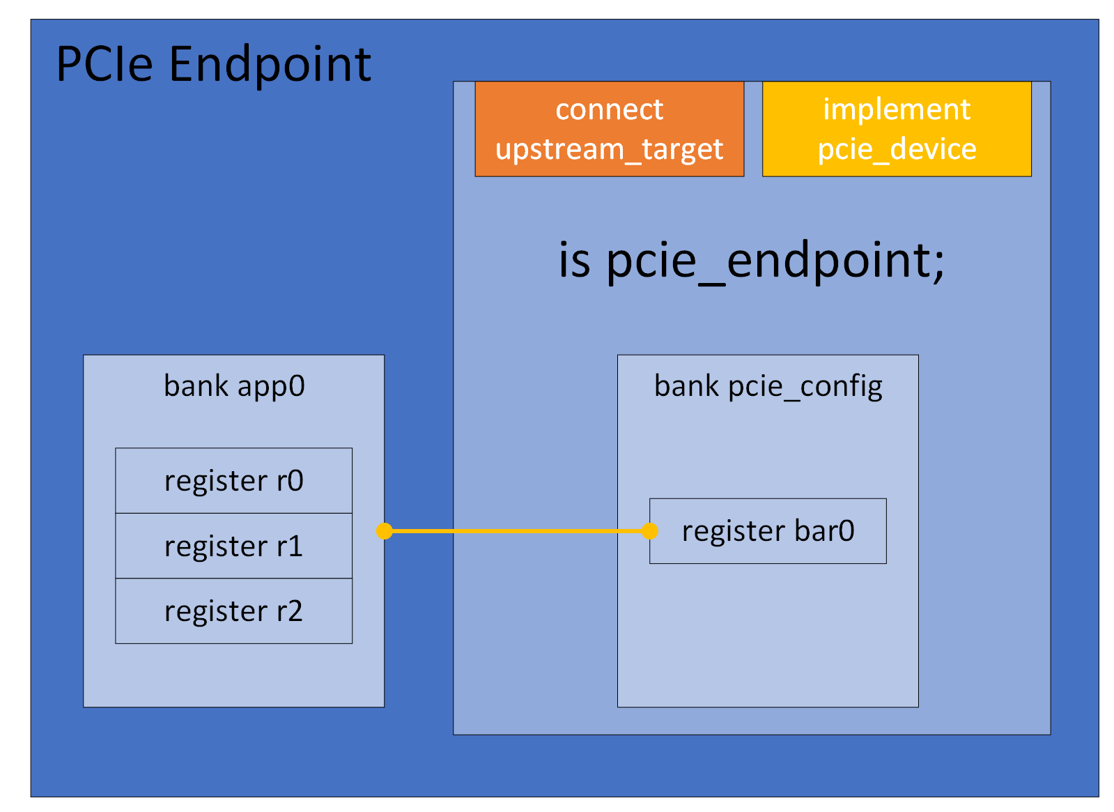
The configuration header of a PCIe device is a register bank,
typically named pcie_config, which uses the template
physical_config_bank. A register bank would normally
not instantiate this template directly, but use either of
type_0_bank or type_1_bank instead. An
endpoint that uses the pcie_endpoint template automatically gets a
bank pcie_config which is an instance of the
type_0_bank template. All instances of
physical_config_bank will be mapped in the
configuration space of the upstream port when the device is connected,
and all base address registers in the bank will be mapped in the
appropriate address space, according to the type. If more than one
instance of physical_config_bank exists in the same device,
i.e. when simulating a multi-function-device, they must be separated
by assigning different values to the parameter function. Sample code
for a simple multi-function endpoint is available in the quick-start
Multi-Function Endpoint section.
The pcie_config bank defines the registers vendor_id, device_id
and class_code. An endpoint must assign init values for these,
according to the specification of the hardware that is to be
simulated. Sample code for setting Vendor ID, Device ID and Class Code
is available in the quick-start Endpoint section.
Depending on the device to be modeled, the init value for other
registers might also need to be customized.
PCIe defines optional "Capabilities" and "Extended
Capabilities". These are available as templates, configurable by
parameters. The templates are designed to be applied on groups, and
all templates require the parameters base and next_ptr to be
defined. The base parameter defines the address of the first
register in the capability structure. The next_ptr defines the base
address of the first address in the next capability structure (or zero
if this is the last capability). For example, the
Endpoint in the quick-start section has the
Subsystem ID (SSID) and Message Signaled Interrupts (MSI) capabilities
defined
Note that except where explicitly noted, the capability templates just define the registers and fields from the PCIe specification. The actual functionality must then be implemented by the device code. See DML Template Reference for more details.
An endpoint typically defines at least one base address register. In
Simics these are declared by creating registers in the bank that
corresponds to the configuration header (typically pcie_config).
The base address registers must use one of the base address templates,
for example the memory_base_address. The
Endpoint in the quick-start section defines two
Memory Base Address registers, bar0 and bar2. Each of them is tied
to a register bank that will be mapped when the Memory Space Enable
bit in the Command register is written as '1'.
There are a number of different templates that can be used to simulate base address registers, and they can be customized using various parameters. These are described in the Common Templates section of this document.
Endpoints can send legacy interrupts using the
raise_legacy_interrupt and lower_legacy_interrupt methods in the
pcie_config bank. If the Endpoint has MSI or MSI-X capability, it
can use the appropriate Capabilities template implement this and
send message signalled interrupts by using the raise method in the
group using the msi_capability or msix_capability template. The
Endpoint in the quick-start section, for example,
has MSI capability and raises MSI vector 0 when the intr register in
app0 is written.
Simics PCIe uses the transaction_t data type for all
transactions. The config_bank template provides utility
methods for reading and writing to the PCIe memory space. These
methods reside in the group memory and operate on the
upstream_target. Details are available in the
Memory methods section of this document. Below is a
sample DML device which defines a method that reads 8 bytes from PCIe
memory and writes it back with all bits flipped.
dml 1.4;
device endpoint;
import "pcie/common.dml";

is pcie_endpoint;

method process_data(uint64 address) {
    local (pcie_error_t err, uint64 value) = pcie_config.memory.read(addr, 8);
    if (err != PCIE_Error_No_Error) {
        log error: "failed to read PCIe memory @ 0x%x", address;
        return;
    }
    err = pcie_config.memory.write(addr, ~value, 8);
    if (err != PCIE_Error_No_Error)
        log error: "failed to write PCIe memory @ 0x%x", address;
}
Just like for memory transactions, the config_bank
template defines a group message with utility methods for sending
and receiving messages. By default, the methods for receiving just log
an "unimpl" string and return false, indicating that the device did
not accept the message. Device code must override the methods for the
messages it wishes to service, and return true if the message is
accepted. As with the memory group, the methods for sending messages
operate on upstream_target.
Here is a sample DML device which accepts 'Vendor Defined Type 0' messages and sends a 'Vendor Defined Type 1' message upstream, with the address bits inverted. The available methods are described in more detail in the Sending and Receiving Messages sections.
dml 1.4;
device endpoint;
import "pcie/common.dml";

is pcie_endpoint;

bank pcie_config {
    // ...
    group message {
        method vendor_defined_type_0(transaction_t *t, uint64 addr) -> (bool) {
            log info, 2: "VDM Type 0 received, address: 0x%x", addr;
            local pcie_error_t err = message.send(
                ~addr, PCIE_Vendor_Defined_Type_1, PCIE_Msg_Route_Upstream);
            return err == PCIE_Error_No_Error;
        }
    }
    // ..
}
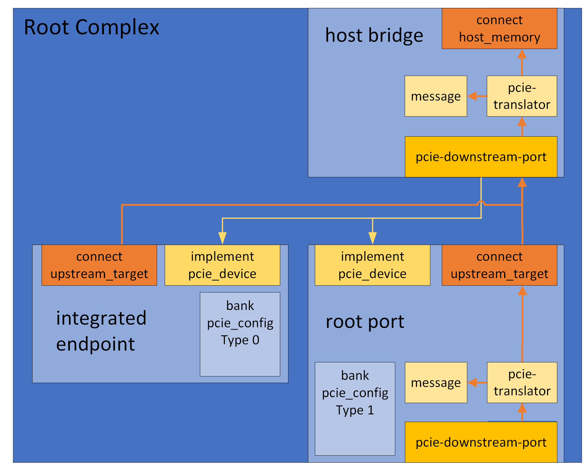
A PCIe device that is not an endpoint, i.e. a Root Port or a a Switch
Port, is simulated with the help of an object of the class
pcie-downstream-port.
A root or switch port would typically use the
pcie_root_port template. The pcie_root_port template
creates a port object downstream_port of the class
pcie-downstream-port and defines a bank pcie_config which is an
instance of the type_1_bank template. It also defines a
connect to an upstream target and provides default implementations for
the interface transaction_translator to handle upstream
transactions.
The type_1_bank template automatically handles the standard base address registers for IO, Memory, and Prefetchable memory. It maps the configured ranges in the appropriate address space of the connected upstream target, forwarding them to its downstream port. Here is an overview image of a sample RC with one root port and one Root Complex Integrated Endpoint (RCiEP)
And here is an overview image of a sample Switch with one upstream and three downstream ports.
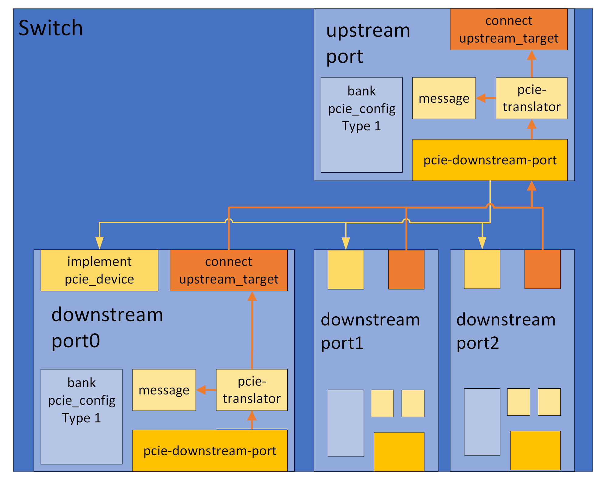
The quick-start section contains sample code for creating a similar Root Complex and Switch
The pcie_root_port automatically forwards all upstream traffic to
its upstream_target. A port that wishes to change that can either
redirect traffic of a certain type by setting any or all of the
parameters def, msg, mem, io, and cfg in the group txl to
a valid map target. Setting it to NULL will block upstream traffic
of that type. See the documentation for the
pcie_translator template for more information.
Messages can be handled by creating instances of the template
handling_messages in the upstream_message port. This port is
created automatically by the pcie_root_port template. See the
documentation for the handling_messages template for more
information. Here is an example that handles Vendor Defined Message
Type 0:
dml 1.4;
device rp;
import "pcie/common.dml";

is pcie_root_port;

port upstream_message {
    group vdm0 is handling_messages {
        method message(transaction_t *t, uint64 addr,
                       pcie_message_type_t type) -> (pcie_error_t) {
            if (type != PCIE_Vendor_Defined_Type_0) {
                // message not handled here
                return PCIE_Error_Not_Set;
            }

            log info: "VDM0 received";
            return PCIE_Error_No_Error;
        }
    }
}
A device that wishes to bridge PCIe to/from host memory, without
necessarily being a Type 1 device, would use the pcie_bridge
template. Like pcie_root_port, the template creates a port object
downstream_port but it doesn't create any register bank and instead
of an upstream_target it has a connect host_memory to which it
translates requests.
Segment routing across PCIe hierarchies is supported in PCIe 6 and the PCIe modeling library provides templates and methods to support it.
Segment routing consists of two parts:
The first part requires as per PCIe 6 specification that configuration requests
contain the segment number for the hierarchy. It is up to the root complex
to append ATOM_transaction_pcie_destination_segment atom to downstream
configuration requests. The PCIe library will capture this atom and store
its value internally. This is true for Root Ports, Switches and Endpoints.
For segment routing to work all relevant devices in the hierarchy must instantiate
the dev3_capability capability. For instance if an endpoint wants to route a message
to a target that is part of another PCIe hierarchy all upstream ports connecting
the endpoints to the Root Complex must have the dev3_capability instantiated.
The second part is handled automatically within the PCIe library up until the Root Complex.
But first the message initiator must setup the message transfer utilizing
the send_custom method. More details in the Sending
Message section.
dml 1.4;
device endpoint;
import "pcie/common.dml";

is pcie_endpoint;

bank pcie_config {
    // ...
    is defining_dev3_capability;
    param dev3_offset = 0x100;
    param dev3_next_ptr = dev3_offset + 0x100;
    // ..

    method send_message(uint16 target_id, uint8 segment_number) {
        local atom_t extra_atoms[2];

        extra_atoms[0] = ATOM_pcie_destination_segment(segment_number);
        extra_atoms[1] = ATOM_list_end(0);
        local bytes_t data;

        local pcie_error_t ret = message.send_custom(target_id << 48,
                                                    PCIE_Vendor_Defined_Type_0,
                                                    PCIE_Msg_Route_ID,
                                                    data,
                                                    extra_atoms);
    }
}
dml 1.4;
device root_complex;
import "utility.dml";
import "pcie/common.dml";

param pcie_version = 6.0;

param nbr_segments = 4;

group segment[segment_id < nbr_segments] {
    subdevice bridge is pcie_bridge {
        group txl_target {
            param msg = dev.upstream_messages.map_target;
        }
    }
    subdevice root_port is (pcie_root_port, post_init) {
        bank pcie_config {
            register capabilities_ptr {
                param init_val = 0x40;
            }
            is defining_pm_capability;
            param pm_offset = capabilities_ptr.init_val;
            param pm_next_ptr = pm_offset + 0x10;

            is defining_exp_capability;
            param exp_offset = pm_next_ptr;
            param exp_next_ptr = exp_offset + 0x30;
            param exp_dp_type = PCIE_DP_Type_RP;

            is defining_dev3_capability;
            param dev3_offset = exp_next_ptr;
            param dev3_next_ptr = dev3_offset + 0x100;
        }
        method post_init() {
            pcie_device.connected(bridge.downstream_port.obj, 0);
        }
    }
}
port upstream_messages is (init_mt) {
    implement transaction_translator {
        method translate(uint64 addr,
                         access_t access,
                         transaction_t *t,
                         exception_type_t (*callback)(translation_t txl,
                                                      transaction_t *tx,
                                                      cbdata_call_t cbd),
                         cbdata_register_t cbdata) -> (exception_type_t) default {
            local pcie_msg_route_t route =
                ATOM_get_transaction_pcie_msg_route(t);
            local const uint8* seg_id =
                ATOM_transaction_pcie_destination_segment(t);

            local translation_t txl;
            switch (route) {
            case PCIE_Msg_Route_ID:
                if (seg_id != NULL && *seg_id < nbr_segments) {
                    txl.target = segment[*seg_id].bridge.downstream_port.map_target;
                }
                break;
            case PCIE_Msg_Route_Upstream:
                txl.target = dev.message.map_target;
                break;
            default:
                log error: "%s, Unexpected pcie routing type: %d", this.qname, route;
                return Sim_PE_IO_Not_Taken;
            }
            if (txl.target) {
                log info, 2:
                    "Forwarding messages: %s, %s, segment=%d, address=0x%x, to: %s",
                    pcie_message_type_name(ATOM_get_transaction_pcie_msg_type(t)),
                    pcie_route_type_name(ATOM_get_transaction_pcie_msg_route(t)),
                    *seg_id,
                    addr,
                    SIM_object_name(SIM_map_target_object(txl.target));
            }
            return callback(txl, t, cbdata);
        }
    }
}

port message is (message_port);
The template pcie_phy adds a port to a device with the name phy. This is
intended to be used as a target for transactions which are related to the
physical layer in PCIe. The current default transaction handler in this port
handles transactions that contain the pcie_link_negotiation atom. It will try
to do link training by comparing the incoming max speed/width with its own max
speed/width and let the transaction initiator know the maximum common value of
the respective property. This is essentially a simplification of the T1 and T2
ordered sets that are actually communicated in a real PCIe link. Transactions in
this layer are expected to have a BDF in address[31:16]. The bus number is
unused as the transactions only traverse over one link. The function is
currently also unused as the transaction will end up in the top-level of a
device.
Take the standard PCIe switch distributed as part of Simics Base. It indicates
support of link speeds and widths using extended capability structures.
Additionally, the supported values have been set in the link registers of the
PCI Express Capability Structure. It also supports Hot-Plug along with having
an attention button and a power indicator. The latter two are useful for
Hot-Plug removal and software reporting status of Hot-Plug operations. Support
for these features are enabled using params found in the exp_capability and
exp_slot templates. This will result in the device emitting interrupts for
Slot and Link related events if software has enabled it. In the case where
interrupts might be generated by firmware in the device rather by hardware in
the device, shared methods found in the exp_slot template can be overridden to
fit a certain use case.
dml 1.4;

device standard_pcie_switch;
param classname = "standard-pcie-switch";

param desc = "standard PCIe switch";

param documentation = "A standard PCIe switch with 4 downstream slots that"
                    + " contains the mandatory capabilities for a PCIe"
                    + " function in all ports.";

import "pcie/common.dml";

param pcie_version = 6.0;


template switch_port {
    bank pcie_config {
        register device_id { param init_val = 0x0370; }
        register vendor_id { param init_val = 0x8086; }
        register capabilities_ptr { param init_val = 0x40; }

        register bar0 @ 0x10 is (memory_base_address_32) {
            param size_bits = 14;
        }

        is defining_pm_capability;
        param pm_offset = capabilities_ptr.init_val;
        param pm_next_ptr = pm_offset + 0x08;

        is defining_msix_capability;
        param msix_offset = pm_next_ptr;
        param msix_next_ptr = msix_offset + 0x0C;
        param msix_num_vectors = 32;
        param msix_table_offset_bir = 0;
        param msix_pba_offset_bir = (0x10 * msix_num_vectors) << 3;
        param msix_data_bank = msix_data;

        is defining_exp_capability;
        param exp_offset = msix_next_ptr;
        param exp_next_ptr = 0xFF;
        group exp {
            param has_links = true;
            group link {
                param max_link_speed = PCIE_Link_Speed_32;
                param max_link_width = PCIE_Link_Width_x8;
            }
        }

        is defining_dlf_capability;
        param dlf_offset = 0xFF;
        param dlf_next_ptr = dlf_offset + 0x0C;
        is defining_pl16g_capability;
        param pl16g_offset = dlf_next_ptr;
        param pl16g_next_ptr = pl16g_offset + 0x28;
        param pl16g_max_link_width = PCIE_Link_Width_x8;
        param pl16g_max_lanes = PCIE_Link_Width_x8;
        is defining_pl32g_capability;
        param pl32g_offset = pl16g_next_ptr;
        param pl32g_next_ptr = 0;
        param pl32g_max_lanes = PCIE_Link_Width_x8;
    }

    bank msix_data is msix_table {
        param msix_bank = pcie_config;
    }
}

subdevice usp is (pcie_upstream_port, switch_port) {
    bank pcie_config {
        param exp_dp_type = PCIE_DP_Type_UP;
    }
}

subdevice dsp[i < 4] is (pcie_downstream_port, pcie_link_training,
                         switch_port, post_init) {
    bank pcie_config {
        param exp_dp_type = PCIE_DP_Type_DP;

        group exp {
            param has_hotplug_capable_slot = true;
            param has_attention_button_slot = true;
            group slot {
                param has_power_indicator = true;
            }
        }
    }


    method post_init() {
        pcie_device.connected(usp.downstream_port.obj, i << 3);
    }
}
Note that the downstream ports also have to instantiate the template
pcie_link_training for link training support. This will ensure that when a
device is connected, link training will be initiated to the device on the other
side of the link. For link training to be successful, the device on the other
side of the link also has to have a function(s) that contain link attributes in
their PCIe Express Capability Structure (for example by setting the params
max_link_speed and max_link_width in the link group) as done for the switch
in the example above.