Simics provides a set of DML templates to assist in writing models for
PCIe compliant devices. The templates are available in
[simics]/src/devices/dml-lib/pcie/.
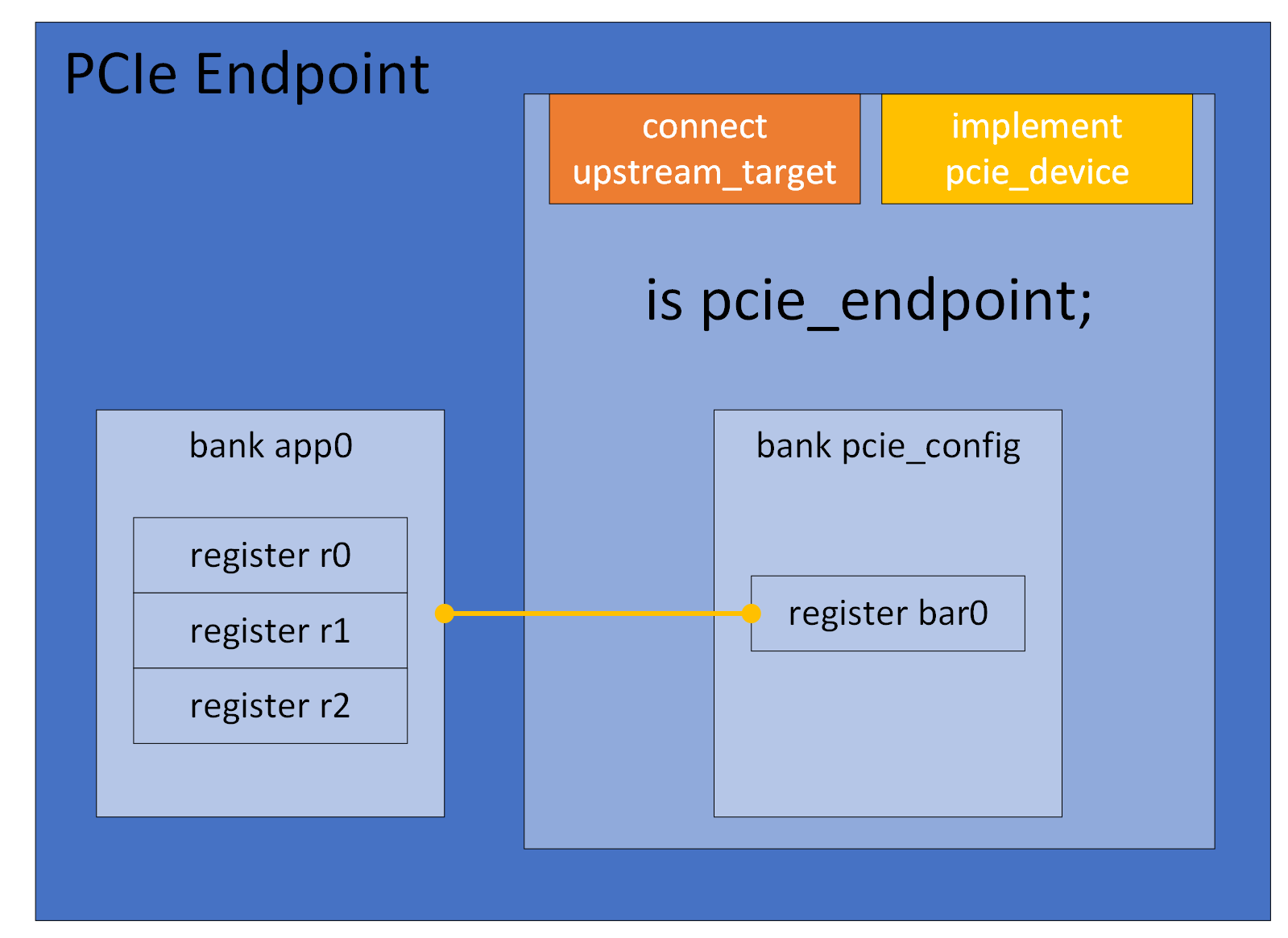
A typical endpoint device would use the pcie_endpoint
template. This template defines the pcie_config register bank which
simulates a Type 0 Configuration header. It also defines a connect for
the upstream target, implements the required interfaces, and handles the
mapping of resources defined in any base address registers. When using
the template, all PCIe access types (memory, IO, configuration, or message)
will enter the device via the port upstream_ingress. The port will then
route the transactions to their respective destinations: the pcie_config
bank for configuration or message transactions, or the Memory/IO BAR-mapped
resources. This port allows to handle all incoming traffic before
it takes any effect. For example, a powered-down device could terminate all
accesses there. Note that also for multi-function endpoints there is only
one upstream ingress port for the entire device.
The configuration header of a PCIe device is a register bank,
typically named pcie_config, which uses the template
physical_config_bank. A register bank would normally
not instantiate this template directly, but use either of
type_0_bank or type_1_bank instead. An
endpoint that uses the pcie_endpoint template automatically gets a
bank pcie_config which is an instance of the
type_0_bank template. All instances of
physical_config_bank will be mapped in the
configuration space of the upstream port when the device is connected,
and all base address registers in the bank will be mapped in the
appropriate address space, according to the type. If more than one
instance of physical_config_bank exists in the same device,
i.e. when simulating a multi-function-device, they must be separated
by assigning different values to the parameter function. Sample code
for a simple multi-function endpoint is available in the quick-start
Multi-Function Endpoint section.
The pcie_config bank defines the registers vendor_id, device_id
and class_code. An endpoint must assign init values for these,
according to the specification of the hardware that is to be
simulated. Sample code for setting Vendor ID, Device ID and Class Code
is available in the quick-start Endpoint section.
Depending on the device to be modeled, the init value for other
registers might also need to be customized.
PCIe defines optional “Capabilities” and “Extended
Capabilities”. These are available as templates, configurable by
parameters. The templates are designed to be applied on groups, and
all templates require the parameters base and next_ptr to be
defined. The base parameter defines the address of the first
register in the capability structure. The next_ptr defines the base
address of the first address in the next capability structure (or zero
if this is the last capability). For example, the
Endpoint in the quick-start section has the
Subsystem ID (SSID) and Message Signaled Interrupts (MSI) capabilities
defined
Note that except where explicitly noted, the capability templates just define the registers and fields from the PCIe specification. The actual functionality must then be implemented by the device code. See DML Template Reference for more details.
An endpoint typically defines at least one base address register. In
Simics these are declared by creating registers in the bank that
corresponds to the configuration header (typically pcie_config).
The base address registers must use one of the base address templates,
for example the memory_base_address_64. The
Endpoint in the quick-start section defines two
Memory Base Address registers, bar0 and bar2. Each of them is tied
to a register bank that will be mapped when the Memory Space Enable
bit in the Command register is written as ‘1’.
There are a number of different templates that can be used to simulate base address registers, and they can be customized using various parameters. These are described in the Common Templates section of this document.
PCIe functions can send legacy interrupts using the
raise_legacy_interrupt and lower_legacy_interrupt methods in the
pcie_config bank. If the function has an MSI and/or MSI-X capability, it
can use the appropriate Capabilities template to implement this and
send message signalled interrupts by using the raise method in the
group using the msi_capability or msix_capability template. The
Endpoint in the quick-start section, for example,
has MSI capability and raises MSI vector 0 when the intr register in app0 is
written. If a function has both an MSI and an MSI-X capability, it’s important
to either call the raise() method on both capabilities (if the capability is
disabled, it is a no-op), or use the enabled() method on both capabilities to
check which one is enabled before calling the applicable raise() method.
MSI-X is less straightforward compared to MSI. With MSI-X, there is the MSI-X Table and the MSI-X PBA structure that both reside in BAR mapped memory space. The library is able to handle all of this accordingly, but there is more configuration needed compared to MSI where it’s simple to just instantiate the MSI capability template and be done with it.
dml 1.4;
device msix_example_1;
import "pcie/common.dml";

is pcie_endpoint;

bank pcie_config {
    register capabilities_ptr { param init_val = 0x40; }
    // bar is a BAR register at position 1 since it is at offset 0x14
    register bar @ 0x14 is (memory_base_address_64) { param size_bits = 12; }

    is defining_msix_capability;
    param msix_offset = 0x40;
    param msix_next_ptr = 0;
    param msix_num_vectors = 32;
    // The Table and PBA params contains the BIR value at the 3 lower bits and
    // the offset at the remaining 29 bits.
    param msix_table_offset_bir = 1;
    param msix_pba_offset_bir = ((0x10 * msix_num_vectors) << 3) | 1;
    param msix_data_bank = msix_data;
}

// Internal representation of the MSI-X state
bank msix_data is msix_table {
    param msix_bank = pcie_config;
}
Here we have an endpoint with one function that contains an MSI-X capability.
We have set the msix_table_offset_bir param to 1.
This param represents the values Table BIR and Table Offset in the MSI-X capability structure.
Since Table BIR becomes 1, and Table Offset also becomes 0, the MSI-X Table will end up in the memory region mapped by bar (which is at position 1) at offset 0.
With msix_pba_offset_bir set to ((0x10 * msix_num_vectors) << 3) | 1 and (0x10 * msix_num_vectors) being the size of the MSI-X Table, the PBA BIR is also 1.
However, the offset makes the PBA start just after where the Table has ended (in the same memory region).
A few notes:
msix_data, which instantiates msix_table, should not
need any consideration by the user, since this is a library implementation
detail.pcie_config.msix.raise(<vector>).msix_capability is instantiated on an offset which is in line with the BIR
selection for both the Table and the PBA.map_obj param in the BAR register definition) would
start at offset 0 of memory-region mapped by the BAR register. The MSI-X Table
and PBA can have any offset (as long as it does not overlap with valid access
points in the map_obj).Simics PCIe uses the transaction_t data type for all
transactions. The config_bank template provides utility
methods for reading and writing to the PCIe memory space. These
methods reside in the group memory and operate on the
upstream_target. Details are available in the
Memory methods section of this document. Below is a
sample DML device which defines a method that reads 8 bytes from PCIe
memory and writes it back with all bits flipped.
dml 1.4;
device endpoint;
import "pcie/common.dml";

is pcie_endpoint;

method process_data(uint64 address) {
    local (pcie_error_t err, uint64 value) = pcie_config.memory.read(addr, 8);
    if (err != PCIE_Error_No_Error) {
        log error: "failed to read PCIe memory @ 0x%x", address;
        return;
    }
    err = pcie_config.memory.write(addr, ~value, 8);
    if (err != PCIE_Error_No_Error)
        log error: "failed to write PCIe memory @ 0x%x", address;
}
Just like for memory transactions, the config_bank
template defines a group message with utility methods for sending
and receiving messages. By default, the methods for receiving just log
an “unimpl” string and return false, indicating that the device did
not accept the message. Device code must override the methods for the
messages it wishes to service, and return true if the message is
accepted. As with the memory group, the methods for sending messages
operate on upstream_target.
Here is a sample DML device which accepts ‘Vendor Defined Type 0’ messages and sends a ‘Vendor Defined Type 1’ message upstream, with the address bits inverted. The available methods are described in more detail in the Sending and Receiving Messages sections.
dml 1.4;
device endpoint;
import "pcie/common.dml";

is pcie_endpoint;

bank pcie_config {
    // ...
    group message {
        method vendor_defined_type_0(transaction_t *t, uint64 addr) -> (bool) {
            log info, 2: "VDM Type 0 received, address: 0x%x", addr;
            local pcie_error_t err = message.send(
                ~addr, PCIE_Vendor_Defined_Type_1, PCIE_Msg_Route_Upstream);
            return err == PCIE_Error_No_Error;
        }
    }
    // ..
}
As described in section endpoints, all traffic enters the device via the port
upstream_ingress. In order to handle incoming traffic in this port, the
translate method of the transaction_translator interface of the port
needs to be overridden as shown in the below example.
The first log message in the example is where you can inspect the incoming
transaction and possibly route it to other places like a handler for
transactions that arrive when the device is powered down.
In order to let the transaction progress to its default destination,
one needs to call the default implementation of the translate method.
After calling into default the result can be inspected.
port upstream_ingress {
    implement transaction_translator {
        method translate(uint64 addr,
                         access_t access,
                         transaction_t *t,
                         exception_type_t (*callback)(translation_t txl,
                                                      transaction_t *tx,
                                                      cbdata_call_t cbd),
                         cbdata_register_t cbdata) -> (exception_type_t) default {
            log info, 2: "Before calling into target";
            local exception_type_t rv = default(addr, access, t, callback, cbdata);
            log info, 2: "After calling into target";
            return rv;
        }
    }
}
PCIe defines two types of resets: Conventional Reset and FLR (Function Level Reset)
Conventional Reset is divided into three categories: Cold, Warm and Hot
Cold reset in the PCIe library is the same as instantiating the PCIe device in Simics.
Warm reset is modeled in the library.
Hot reset is defined in the PCIe specification and is modeled. FLR is also modeled in the library.
Warm reset is modeled with the hard_reset templates and a HRESET signal port exists to
trigger a warm reset externally. All registers go back to their initial state.
A template conditional_hard_reset is provided for registers and fields that conditionally keep their values across warm reset depending on a run-time predicate.
Hot reset is modeled with the soft_reset templates, (defined in DML Utilities), in the library.
In PCIe Hot reset is triggered by an inband signal.
In Simics the inband signal is modeled through the pcie_device
interface method hot_reset. When an upstream port triggers
this method a soft_reset is invoked on the PCIe device, resetting
each PCIe function below the object implementing the pcie_device
interface. Register fields inheriting template pcie_sticky
are not affected by a Hot reset. The library adds the template pcie_sticky
to all fields defined as sticky in the specification.
A template conditional_soft_reset is provided for registers and fields that conditionally keep their values across hot reset depending on a run-time predicate.
FLR only applies to Endpoints and is modeled with the pcie_function_level_reset templates
in the library. FLR operates on function level.
Firmware can reset individual functions in a multi function device by invoking FLR.
Each type_0_bank inherits template pcie_function_level_reset.
Firmware invokes an FLR by writing 1 to field bcre_iflr in the
Device Control Register or to field iflr in the Control register in the PCI AF capability.
An FLR is initiated by invoking method pcie_function_level_reset on the function’s PCIe config bank.
It causes all FLR relevant fields to reset to their initial state and resets relevant states
within the PCIe device.
To add custom FLR logic to a model the user has to override the pcie_function_level_reset method
in the bank.
dml 1.4;
device endpoint;
import "pcie/common.dml";

saved int my_function_state;

is pcie_endpoint;
bank pcie_config {
    register capabilities_ptr {
        param init_val = 0x40;
    }

    is defining_exp_capability;
    param exp_offset = capabilities_ptr.init_val;
    param exp_next_ptr = 0x0;
    param exp_dp_type = PCIE_DP_Type_EP;

    method pcie_function_level_reset() {
        default();
        log info, 2: "Resetting function";
        my_function_state = 0;
    }
}
A template conditional_pcie_function_level_reset is provided for registers and fields that conditionally keep their values across FLR depending on a run-time predicate.
To add custom reset logic that needs to be run for all PCIe resets: Warm, Hot and FLR,
one should utilize the pcie_after_reset method at the top of the PCIe config bank. It
will by default be invoked by all PCIe reset types.
dml 1.4;
device endpoint;
import "pcie/common.dml";

is pcie_endpoint;
bank pcie_config {
    saved int state;
    method pcie_after_reset() {
        default();
        log info, 2: "Resetting model";
        state = 0;
    }
}
The pcie_config bank has a parameter use_standard_access_templates that
defaults to true. When this parameter is set to true,
the library automatically adds templates read_only, hwinit and ignore_write
to registers and fields according to PCIe specification.
The hwinit template by default makes the field read-only. See
DML Template Reference for more details for the hwinit template.
The actual implementation of HwInit in vendor hardware implementations
varies because the PCIe specification states that the Hwinit behaviour is vendor
defined to a large extent. Therefore the HwInit behaviour in the lib can be tailored
to accommodate vendor functionality.
Here are a few examples of HwInit hardware behaviour which the library can model:
dml 1.4;
device endpoint;
import "pcie/common.dml";

is pcie_endpoint;
bank pcie_config {
    in each (hwinit) {
        param writable_after_hreset = true;
    }
}
dml 1.4;
device endpoint;
import "pcie/common.dml";

is pcie_endpoint;

bank pcie_config {
    in each (hwinit) {
        param writable_once_only = false;
    }
}
port hwinit_control_signal is signal_port {
    implement signal {
        method signal_raise() {
            default();
            pcie_config.unlock_hwinit_registers();
        }
        method signal_lower() {
            default();
            pcie_config.lock_hwinit_registers();
        }
    }
}
dml 1.4;
device endpoint;
import "pcie/common.dml";

is pcie_endpoint;

bank pcie_config {
    in each (hwinit) {
        param writable_after_hreset = true;
        param writable_once_only = false;
    }
}
The templates conditional_hard_reset, conditional_soft_reset and conditional_pcie_function_level_reset facilitate modeling registers and fields that conditionally keep their value across the respective reset depending on a run-time predicate.
This is used in the Power Management capability to model Power Management Event bits.
Those are only sticky across reset if the respective bit is set in the PM Capabilities register.
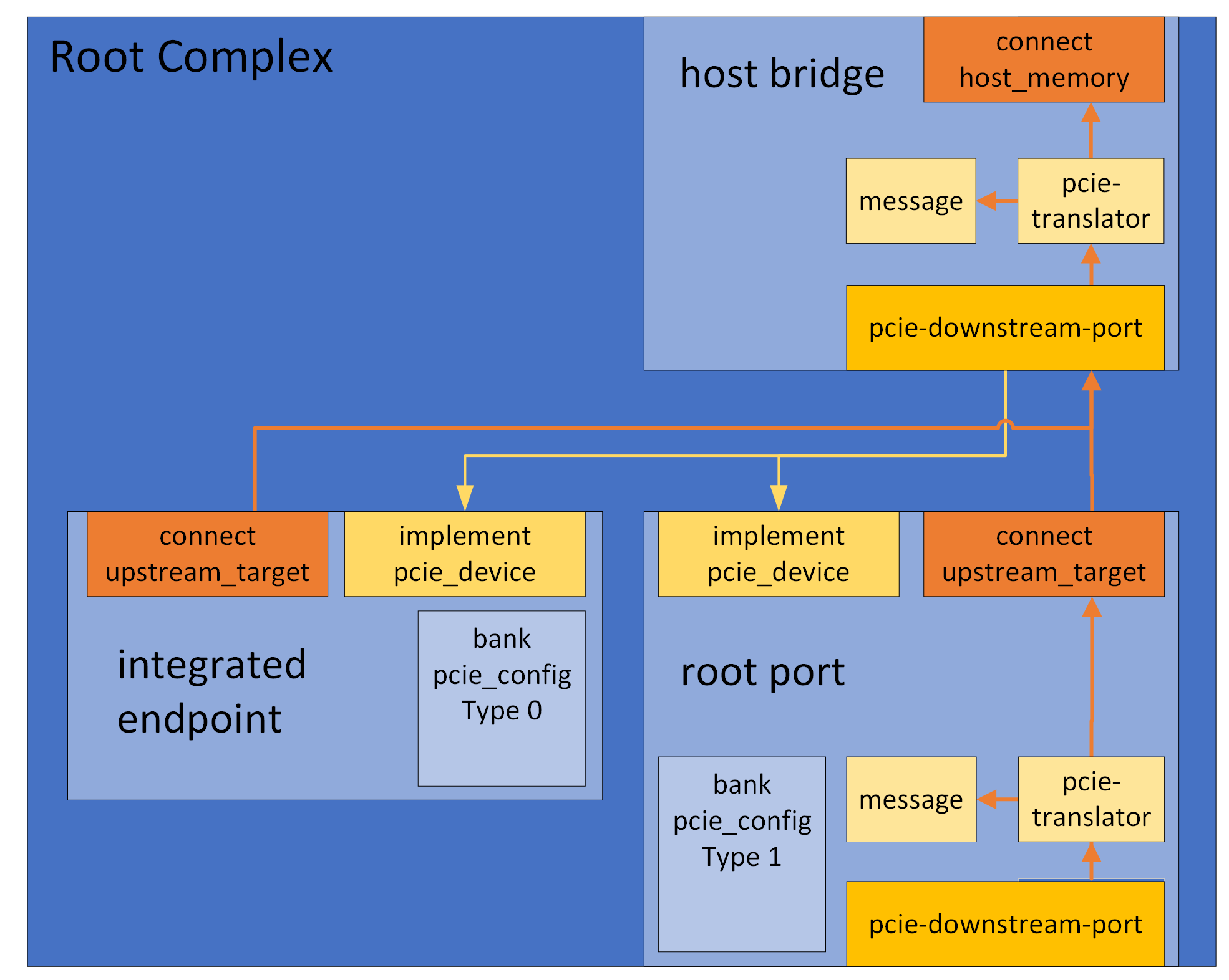
A PCIe device that is not an endpoint, i.e. a Root Port or a Switch
Port, is simulated with the help of an object of the class
pcie-downstream-port.
A root or switch port would typically use one of the
pcie_root_port, pcie_downstream_port or
pcie_upstream_port templates (an object that instantiates one of
these templates will from now be referenced as a PCIe port). These PCIe port
templates create a port object downstream_port of the class
pcie-downstream-port and defines a bank pcie_config which is an instance of
the type_1_bank template. It also defines a connect to an
upstream target and provides default implementations for the interface
transaction_translator to handle upstream transactions. PCIe ports are also
constructed with an upstream_ingress port that all downstream transactions
flow through. Similar to endpoints the upstream_ingress routes transactions
to internal resources in the PCIe port, but for PCIe ports the
upstream_ingress port also manages downstream routing to the port’s secondary bridge.
The type_1_bank template automatically handles the standard base address registers for IO, Memory, and Prefetchable memory. It maps the configured ranges in the appropriate address space of the connected upstream target, forwarding them to its downstream port. Here is an overview image of a sample RC with one root port and one Root Complex Integrated Endpoint (RCiEP).
And here is an overview image of a sample Switch with one upstream and three downstream ports.
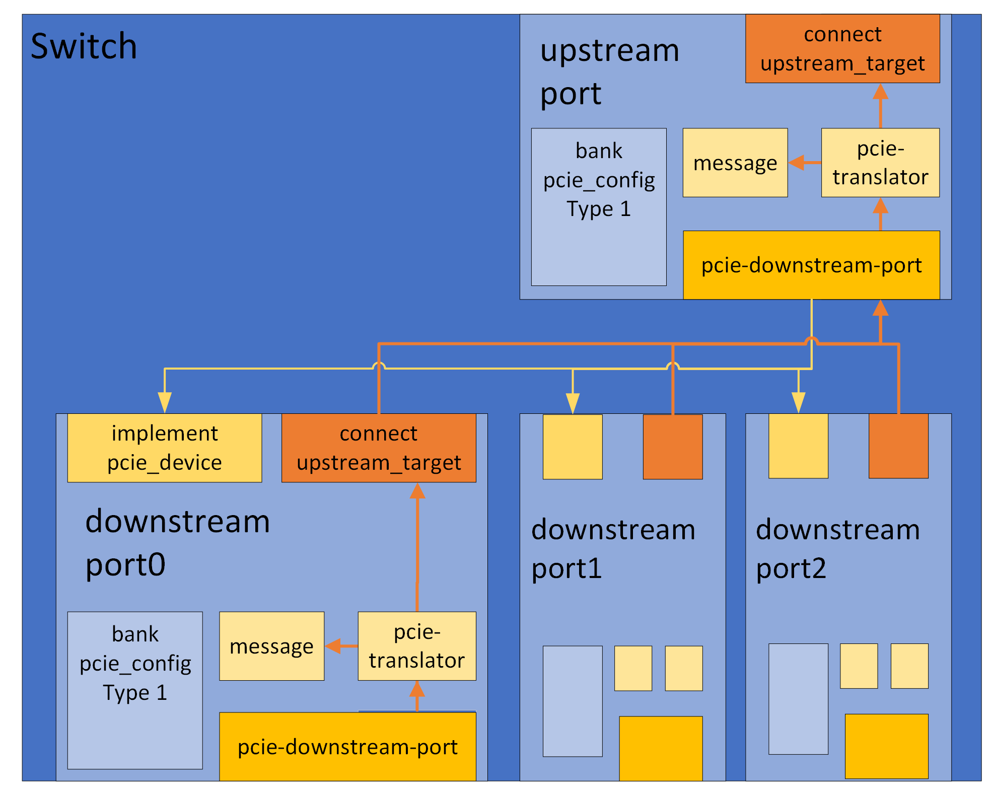
The quick-start section contains sample code for creating a similar Root Complex and Switch
A PCIe port by default automatically forwards all downstream traffic to its
pcie-downstream-port helper object. Since the PCIe port is also based on the
pcie_device template, all the traffic will first go through its
upstream_ingress port before hitting the pcie-downstream-port.
By overriding the transaction_translator in the upstream ingress port,
a PCIe port can dynamically redirect downstream traffic, apply custom access
restrictions or add atoms to a downstream transaction. See the
section about adding atoms to a
transaction if applicable.
Adding atoms to a transaction by chaining multiple transactions needs to be handled with care if the object that adds the atom does not want break support for deferred transactions in a platform that supports it. More information regarding this topic can be found here, which is an important read to understand the example below.
In the example below, the transaction_translator interface of the
upstream_ingress port in an object that has instantiated the
pcie_root_port template has been overridden. Here, if the transaction is a
memory transaction and has an address of 0x3cc00004, the pcie_ecs atom is
added to the transaction by chaining transactions.
Note that to maintain support for checkpointing in the
presence of deferred transactions, the value of the pcie_ecs atom along with
the transaction id is stored in an attribute chained_transactions. It also has
to been ensured that when the checkpoint is read, the deferred transactions are
restored, as seen in the set() method of the attribute.
port upstream_ingress {
    implement transaction_translator {
        method translate(uint64 addr,
                        access_t access,
                        transaction_t *prev,
                        exception_type_t (*callback)(translation_t txl,
                                                    transaction_t *tx,
                                                    cbdata_call_t cbd),
                        cbdata_register_t cbdata) -> (exception_type_t) {
            local const pcie_type_t * type = ATOM_transaction_pcie_type(prev);
            if (type != NULL && *type == PCIE_Type_Mem) {
                local translation_t txl = { .target = upstream_ingress_targets.memory.map_target, ... };
                local transaction_t t;

                local int num_atoms = (addr == 0x3cc00004) ? 4 : 3;
                local atom_t atoms[(addr == 0x3cc00004) ? 4 : 3];
                atoms[0] = ATOM_owner(dev.obj);
                atoms[1] = ATOM_completion(&empty_completion);
                if (addr == 0x3cc00004) {
                    atoms[2] = ATOM_pcie_ecs(PCIE_ECS_SIG_OS);
                    atoms[3] = ATOM_list_end(0);
                } else {
                    atoms[2] = ATOM_list_end(0);
                }

                t.atoms = atoms;
                t.prev = prev;

                local exception_type_t exc = callback(txl, &t, cbdata);
                if (exc == Sim_PE_Deferred) {
                    local transaction_t *new_ct = new transaction_t;
                    local atom_t *new_atoms = new atom_t[4];
                    new_ct->atoms = new_atoms;

                    memcpy(new_ct->atoms, t.atoms, sizeof(atoms));
                    new_ct->atoms[1] = ATOM_completion(&completion);
                    new_ct->prev = t.prev;
                    SIM_replace_transaction(&t, new_ct);
                    VADD(chained_transactions.val, new_ct);
                    return SIM_monitor_chained_transaction(new_ct, exc);
                } else {
                    // Cannot return exc directly here. If the parent transaction_t
                    // has a completion atom that it expects to be called,
                    // it will only be called if SIM_monitor_chained_transaction
                    // is called by this transaction.
                    return SIM_monitor_chained_transaction(&t, exc);
                }
            }
            return default(addr, access, prev, callback, cbdata);
        }
    }
}

method empty_completion(transaction_t *t, exception_type_t e) ->
    (exception_type_t) {
    return e;
}

method completion(transaction_t *t, exception_type_t e) ->
    (exception_type_t) {;
    VREMOVE_FIRST_MATCH(chained_transactions.val, t);
    delete t->atoms;
    delete t;
    return e;
}

attribute chained_transactions is destroy {
    param type = "[[ii]*]";
    session transaction_t * vect val;
    param internal = true;

    method set(attr_value_t value) throws {
        if (!SIM_is_restoring_state(obj)) {
            SIM_attribute_error("must only be set during checkpoint restore");
            throw;
        }

        for (local int i = 0; i < VLEN(this.val); i++)
            delete this.val[i];

        VFREE(this.val);

        for (local int i = 0; i < SIM_attr_list_size(value); i++) {
            local attr_value_t li = SIM_attr_list_item(value, i);
            local int64 id = SIM_attr_integer(SIM_attr_list_item(li, 0));
            local pcie_ecs_t ecs = SIM_attr_integer(SIM_attr_list_item(li, 1));

            local transaction_t *t = new transaction_t;
            local atom_t *atoms = new atom_t[ecs != PCIE_ECS_Legacy ? 4 : 3];
            t->atoms = atoms;
            atoms[0] = ATOM_owner(dev.obj);
            atoms[1] = ATOM_completion(&completion);
            if (ecs != PCIE_ECS_Legacy) {
                atoms[2] = ATOM_pcie_ecs(ecs);
                atoms[3] = ATOM_list_end(0);
            }
            else {
                atoms[2] = ATOM_list_end(0);
            }

            VADD(this.val, t);
            SIM_reconnect_transaction(t, id);
        }
    }

    method get() -> (attr_value_t) {
        local attr_value_t value = SIM_alloc_attr_list(VLEN(this.val));
        local transaction_t t;
        for (local int i = 0; i < VLEN(this.val); i++) {
            // connect the atom-list to an empty transaction, to avoid finding
            // atoms in chained 'prev'
            t.atoms = this.val[i]->atoms;
            local attr_value_t li = SIM_make_attr_list(
                2,
                SIM_make_attr_uint64(SIM_get_transaction_id(this.val[i])),
                SIM_make_attr_uint64(ATOM_get_transaction_pcie_ecs(&t)));
            SIM_attr_list_set_item(&value, i, li);
        }
        return value;
    }

    method destroy() {
        // Deferred transactions are completed by Simics Core, we just need to
        // free the vect
        VFREE(this.val);
    }
}
A PCIe port by default automatically forwards all upstream traffic to its
upstream_target. A PCIe port that wishes to change that can either redirect
traffic of a certain type by setting any or all of the parameters def, msg,
mem, io, and cfg in the txl_target group (of the object that
instantiated any of the PCIe port templates) to a valid map target. Setting it
to NULL will block upstream traffic of that type. If a PCIe port wants to
dynamically redirect upstream traffic, the transaction_translator
implementation that is implemented in the PCIe port can instead be be
overridden. See the documentation for the
pcie_upstream_translator template for more information.
Messages can be handled by creating instances of the template
handling_messages in the upstream_message port. This port is
created automatically by the pcie_root_port template. See the
documentation for the handling_messages template for more
information. Here is an example that handles Vendor Defined Message
Type 0:
dml 1.4;
device rp;
import "pcie/common.dml";

is pcie_root_port;

port upstream_message {
    group vdm0 is handling_messages {
        method message(transaction_t *t, uint64 addr,
                       pcie_message_type_t type) -> (pcie_error_t) {
            if (type != PCIE_Vendor_Defined_Type_0) {
                // message not handled here
                return PCIE_Error_Not_Set;
            }

            log info: "VDM0 received";
            return PCIE_Error_No_Error;
        }
    }
}
A device that wishes to bridge PCIe to/from host memory, without
necessarily being a Type 1 device, would use the pcie_bridge
template. Like pcie_root_port, the template creates a port object
downstream_port but it doesn’t create any register bank and instead
of an upstream_target it has a connect host_memory to which it
translates requests.
Segment routing across PCIe hierarchies is supported in PCIe 6 and the PCIe modeling library provides templates and methods to support it.
Segment routing consists of two parts:
The first part requires as per PCIe 6 specification that configuration requests
contain the segment number for the hierarchy. It is up to the root complex
to append ATOM_transaction_pcie_destination_segment atom to downstream
configuration requests. The PCIe library will capture this atom and store
its value internally. This is true for Root Ports, Switches and Endpoints.
For segment routing to work all relevant devices in the hierarchy must instantiate
the dev3_capability capability. For instance if an endpoint wants to route a message
to a target that is part of another PCIe hierarchy all upstream ports connecting
the endpoints to the Root Complex must have the dev3_capability instantiated.
The second part is handled automatically within the PCIe library up until the Root Complex.
But first the message initiator must setup the message transfer utilizing
the send_custom method. More details in the Sending
Message section.
dml 1.4;
device endpoint;
import "pcie/common.dml";

is pcie_endpoint;

bank pcie_config {
    // ...
    is defining_dev3_capability;
    param dev3_offset = 0x100;
    param dev3_next_ptr = dev3_offset + 0x100;
    // ..

    method send_message(uint16 target_id, uint8 segment_number) {
        local atom_t extra_atoms[2];

        extra_atoms[0] = ATOM_pcie_destination_segment(segment_number);
        extra_atoms[1] = ATOM_list_end(0);
        local bytes_t data;

        local pcie_error_t ret = message.send_custom(target_id << 48,
                                                    PCIE_Vendor_Defined_Type_0,
                                                    PCIE_Msg_Route_ID,
                                                    data,
                                                    extra_atoms);
    }
}
dml 1.4;
device root_complex;
import "utility.dml";
import "pcie/common.dml";

param pcie_version = 6.0;

param nbr_segments := 4;

group segment[segment_id < nbr_segments] {
    subdevice bridge is (pcie_bridge, post_init) {
        group txl_target {
            param msg = dev.upstream_messages.map_target;
        }

        method post_init() {
            local set_error_t ret;
            local attr_value_t rp = SIM_make_attr_list(3, SIM_make_attr_uint64(0),
                                    SIM_make_attr_uint64(0),
                                    SIM_make_attr_object(root_port.obj));
            local attr_value_t root_ports = SIM_make_attr_list(1, rp);

            ret = SIM_set_attribute(downstream_port.obj, "devices", &root_ports);
            SIM_attr_free(&root_ports);
            assert(ret == Sim_Set_Ok);
        }
    }
    subdevice root_port is (pcie_root_port) {
        bank pcie_config {
            register capabilities_ptr {
                param init_val = 0x40;
            }
            is defining_pm_capability;
            param pm_offset = capabilities_ptr.init_val;
            param pm_next_ptr = pm_offset + 0x10;

            is defining_exp_capability;
            param exp_offset = pm_next_ptr;
            param exp_next_ptr = exp_offset + 0x30;
            param exp_dp_type = PCIE_DP_Type_RP;

            is defining_dev3_capability;
            param dev3_offset = exp_next_ptr;
            param dev3_next_ptr = dev3_offset + 0x100;
        }
    }
}
port upstream_messages is (init_mt) {
    implement transaction_translator {
        method translate(uint64 addr,
                         access_t access,
                         transaction_t *t,
                         exception_type_t (*callback)(translation_t txl,
                                                      transaction_t *tx,
                                                      cbdata_call_t cbd),
                         cbdata_register_t cbdata) -> (exception_type_t) default {
            local pcie_msg_route_t route =
                ATOM_get_transaction_pcie_msg_route(t);
            local const uint8* seg_id =
                ATOM_transaction_pcie_destination_segment(t);

            local translation_t txl;
            switch (route) {
            case PCIE_Msg_Route_ID:
                if (seg_id != NULL && *seg_id < nbr_segments) {
                    txl.target = segment[*seg_id].bridge.downstream_port.map_target;
                }
                break;
            case PCIE_Msg_Route_Upstream:
                txl.target = dev.message.map_target;
                break;
            default:
                log error: "%s, Unexpected pcie routing type: %d", this.qname, route;
                return Sim_PE_IO_Not_Taken;
            }
            if (txl.target) {
                log info, 2:
                    "Forwarding messages: %s, %s, segment=%d, address=0x%x, to: %s",
                    pcie_message_type_name(ATOM_get_transaction_pcie_msg_type(t)),
                    pcie_route_type_name(ATOM_get_transaction_pcie_msg_route(t)),
                    *seg_id,
                    addr,
                    SIM_object_name(SIM_map_target_object(txl.target));
            }
            return callback(txl, t, cbdata);
        }
    }
}

port message is (message_port);
Note! As of PCIe 6.1, DOE protocols are now referred to as DOE features.
Data Object Exchange (DOE) is supported and can be implemented in a device using
the doe_capability template. This template by default implements DOE Discovery
protocol. New protocols can be added easily by adding entries in the doe group
of the doe_capability. The DOE Discovery protocol implementation will detect
and report those accordingly with no modifications to the DOE Discovery
implementation. Below is an example of implementing DOE in a PCIe device with a
custom DOE protocol.
dml 1.4;
device endpoint;
import "pcie/common.dml";

is pcie_endpoint;

bank pcie_config {
    register capabilities_ptr { param init_val = 0x40; }
    is defining_doe_capability;
    param doe_offset = 0x40;
    param doe_next_ptr = doe_offset + 0x100;
    param doe_mailbox_len = 50;
    param doe_interrupt_support = true;
    group doe {
        group protocols {
            group test_protocol is doe_test_protocol {}
        }
    }
}

template doe_test_protocol is doe_protocol {
    param vendor_id = 0x00FF;
    param data_object_type = 1;

    method handle_request(const uint32 *req, uint18 req_len) {
        local uint32 res[3];

        local doe_header_t res_header;
        res_header.vendor_id = vendor_id;
        res_header.data_object_type = data_object_type;
        res_header.length = 3;
        memcpy(res, &res_header, sizeof(res_header));

        res[2] = 0xABCDEF;
        try {
            mailbox.push_buffer(res, sizeof(res) / sizeof(res[0]));
            response_ready(sizeof(res) / sizeof(res[0]));
        } catch {
            response_error();
        }
    }
}
Pushing the response can be done with either the push or the push_buffer
methods of the mailbox. Each handling of a data object must conclude with
either a response_ready(res_len) or response_error() invocation.
There are 3 (in-band) error signaling mechanisms defined in the PCIe specification:
The PCIe library has support for the first two mechanisms to various degrees (as discussed below).
A completion packet in PCIe includes a completion status field in the its
header. This is implemented in the library as an atom pcie_error_ret. The
library sets this in some occasions when handling a request, but it can also be
set by the user of the library in applicable contexts. The requester is then
able to inspect the pcie_error_ret atom to determine if the request was
successful or not.
Error messages are messages sent by functions in the PCIe hierarchy that encounter errors (device specific internal errors or errors defined in the PCIe specification) to the Root Complex (more specifically the applicable root port). These messages could also be sent by root complex integrated endpoints, where they instead would be sent to a Root Complex Event Collector (RCEC) if implemented. Note that the library currently has no functional support for Error Messages being collected by an RCEC.
PCIe functions may utilize the emit_errors group in the config_bank to
submit errors using either emit_errors.submit_correctable_error(),
emit_errors.submit_uncorrectable_error() or
emit_errors.submit_uncorrectable_error_advisory_non_fatal(). The library will
then set the applicable status bits in the PCI configuration header as well as
in the PCI Express Capability Structure:
Additionally, if the PCIe function has a AER capability, applicable fields depending on the error and if software has not masked certain errors in the AER capability:
Root ports will also if instantiating the handling_err_messages without
overriding the default implementation set the following fields in the AER
capability based on values in the Root Error Command register:
If software otherwise has configured the device to send error messages for an error type, and not masked the error the error using AER, the library will send these messages upstream automatically. Root ports would instead send these messages to themselves, as per the PCIe specification.
Root ports (that have instantiated pcie_root_port) may instantiate the
handling_err_messages template in their local message target port (by default
the upstream_message port in the root port). In this instantiation, the
handle_error_message() method can be overridden to handle incoming error
signaling messages coming from downstream functions. The default behavior of
this method is to generate applicable interrupts based on the configuration of
the AER capability (if it has one), which is described earlier in this section.